- 您现在的位置:买卖IC网 > Sheet目录344 > MSC8144ADS (Freescale Semiconductor)ADS FOR MSC8144 DEVICE
2.6.14
JTAG Signals
Table 50. JTAG Timing
All frequencies
Characteristics
Symbol
Min
Max
Unit
TCK cycle time
TCK clock high phase measured at V M = 1.6 V
Boundary scan input data setup time
Boundary scan input data hold time
TCK fall to output data valid
TCK fall to output high impedance
TMS, TDI data setup time
TMS, TDI data hold time
TCK fall to TDO data valid
TCK fall to TDO high impedance
TRST assert time
t TCKX
t TCKH
t BSVKH
t BSXKH
t TCKHOV
t TCKHOZ
t TDIVKH
t TDIXKH
t TDOHOV
t TDOHOZ
t TRST
36.0
15.0
0.0
15.0
—
—
0.0
5.0
—
—
100.0
—
—
—
—
20.0
24.0
—
—
10.0
12.0
—
ns
ns
ns
ns
ns
ns
ns
ns
ns
ns
ns
Note:
All timings apply to OnCE module data transfers as well as any other transfers via the JTAG port.
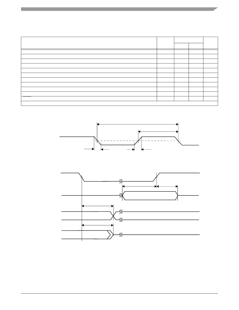
Figure 38 shows the Test Clock Input Timing Diagram
t TCKX
t TCKH
TCK
(Input)
t TCKR
V M
V M
t TCKR
Figure 38. Test Clock Input Timing
Figure 39 shows the boundary scan (JTAG) timing diagram.
TCK
(Input)
t BSVKH
t BSXKH
Data
Inputs
Data
Outputs
t TCKHOV
Input Data Valid
Output Data Valid
t TCKHOZ
Data
Outputs
Figure 39. Boundary Scan (JTAG) Timing
MSC8144 Quad Core Digital Signal Processor Data Sheet, Rev. 16
Freescale Semiconductor
63
发布紧急采购,3分钟左右您将得到回复。
相关PDF资料
MSC8156EVM
EVAL MODULE FOR MSC8156 LC
MSL1060AW
IC LED DRIVER 6 STRING
MSL1061AV
IC LED DRIVER 6 STRING
MSL2041GU
IC LED DRIVER 4 STRING
MSL2100BR
IC LED DRIVER 8 STRING
MSL2160DQ
IC LED DRIVER 16 STRING
MSL2162DQ
IC LED DRIVER 16 STRING
MSL3082CS
IC LED DRIVER 8 STRING
相关代理商/技术参数
MSC8144AMC-SA
制造商:Freescale Semiconductor 功能描述:BOARD AMC SGL WIDTH MSC8144 DSP
MSC8144E
制造商:FREESCALE 制造商全称:Freescale Semiconductor, Inc 功能描述:Quad Core Digital Signal Processor
MSC8144EC
制造商:FREESCALE 制造商全称:Freescale Semiconductor, Inc 功能描述:Quad Core Digital Signal Processor
MSC8144ESVT1000B
制造商:Freescale Semiconductor 功能描述:DSP 32-BIT 1GHZ 1000MIPS 783-PIN FCBGA BOX - Trays 制造商:Freescale Semiconductor 功能描述:ENCRYPTION PACSUN R2.1 783FCPBGA
MSC8144ESVT800A
制造商:Freescale Semiconductor 功能描述:DSP 32BIT 800MHZ 800MIPS 783FCBGA - Trays
MSC8144ESVT800B
制造商:Freescale Semiconductor 功能描述:DSP 32-BIT 800MHZ 800MIPS 783-PIN FCBGA EACH - Bulk 制造商:Freescale Semiconductor 功能描述:ENCRYPTION PACSUN R2.1 783FCPBGA
MSC8144ETVT1000A
制造商:Freescale Semiconductor 功能描述:DSP 32-BIT 1GHZ 1000MIPS 783-PIN FCBGA - Bulk
MSC8144ETVT1000B
制造商:Freescale Semiconductor 功能描述:DSP 32-BIT 1GHZ 1000MIPS 783-PIN FCBGA EACH - Bulk 制造商:Freescale Semiconductor 功能描述:ENCRYPTION PACSUN R2.1 783FCPBGA
